Table Of Content

An op-amp is comprised of an inverting and noninverting input, a positive and negative power rail, and output. Inside the op-amp exists a gain factor, which is a ratio of the output voltage over the input voltage. In an idealized model, the gain is assumed to be infinite; for practical modeling, the gain is provided by the datasheet and helps establish the minimum threshold for boosting the voltage. By running the inverting input to ground through a pulldown resistor and providing a positive or negative voltage on the noninverting input, the voltage is amplified by the gain.
Voltage sources
Analog circuit simulation is a powerful tool that allows the designer to further tune the component values of a schematic before needing to design the layout, which reduces engineering time and work. Finally, layout tools are used to design the printed circuit board (PCB), where the designer can define the component distribution, the routing paths, the number of layers, the vias, the paths, etc. The combination between the schematic, simulation and layout software should be selected wisely, to optimize the design flow. Cost should also be considered, as many design tools are considerably expensive for the average consumer.
Auxiliary and biasing circuits
For example, let consider that we do not have access to a THP210 amplifier, but we have one AD825 (from Analog Devices™) spare in the laboratory. To verify if the AD825 is still able to achieve the filtering properties that we need, we can run a simulation in PSPICE to validate the frequency behavior of the new filter. After the analog design is complete and validated by simulations, the engineer must design the printed circuit board (PCB). Many designers tend to neglect the negative effects caused by poor routing, but this is not the most efficient approach. When developing an electronic project, one should treat the PCB as a crucial component of the circuit, that must be designed carefully to avoid practical problems. Analog design might seem somewhat outdated in the modern world of digital circuits, but it still serves a unique and irreplaceable purpose.
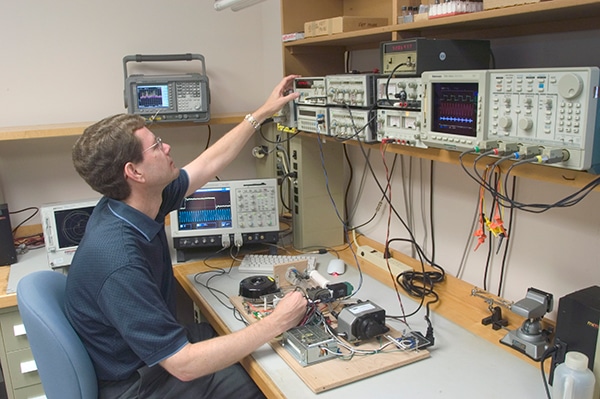
Working with Power Supply Design Tools
Besides frequency and gain, we also established the amount of ripple of the filter. Using this information, one can apply the model equations to figure out the component values. However, this process can be very onerous for complex systems, due to the number of variables and the non-linearity of the equations. Fortunately, for popular circuits, several automatic design tools are available. For instance, the Webench Filter Design Tool, from Texas Instruments™, can output an entire filter design based on the specifications. Using our project requirements, the circuit showed in Figure 9 was generated, as well as a bill of material (BOM) list containing each component value and tolerance.
Designers should be cognizant that data conversion is an analog function, therefore converters should have AGND and DGND pins tied to the AGND plane. This helps reduce introducing noise from the high-speed digital signals into the analog sphere, which would be further propagated through the conversion process. To select the component values, one should use the mathematical model of the circuit to meet the specifications provided.
Sdi Analog Converter Flash Sales atlantaprogressivenews.com - Atlanta Progressive News
Sdi Analog Converter Flash Sales atlantaprogressivenews.com.
Posted: Thu, 25 Apr 2024 23:40:57 GMT [source]
Digital design treats circuit stimulus as a series of discrete logic “ones” and logic “zeros” over time. A logic “one” is typically represented by the presence of the supply voltage for the IC and a logic “zero” is represented by the absence of this voltage (i.e., zero volts). The devices in digital circuits must spend most of their time at either logic “one” or logic “zero”. As long as the circuits processing these signals are consistent in their response to these logic levels, digital design works well.
Keysight, Synopsys, and Ansys Deliver Radio Frequency Design Migration Flow to TSMC's N6RF+ Process Node - StreetInsider.com
Keysight, Synopsys, and Ansys Deliver Radio Frequency Design Migration Flow to TSMC's N6RF+ Process Node.
Posted: Wed, 24 Apr 2024 15:03:34 GMT [source]
Analog Design: Understanding Signals and Applications
BJTs are widely applied in audio amplifiers, MOSFETs are used in switching-mode power supplies, and JFETs are often applied as voltage-controlled resistors. The world of analog design is vast and almost a subdiscipline of PCB design on its own. To efficiently and painlessly handle your analog needs, Cadence’s collection of PCB design and analysis software provides the tools to easily build and incorporate best practices to optimize performance along the way. In short, analog design can heavily utilize a number of op-amp configurations and applications to perform the necessary adaptations of digital circuitry operations. To take a momentary step back from the world of PCB design, sound hobbyist forums have been arguing endlessly over the merits of analog vs. digital since their inception decades ago.
High-speed analog systems will need an alternate method of tying the ground planes, however. Ostensibly, the topic of split ground comes up when discussing mixed-signal designs. Split ground is the concept of dividing the ground between analog and digital components and traces. This has become a PCB topic that tends to attract some less than rigorous best practices for an engineering discipline. This reflexive statement may seem painfully obvious, but it’s worth highlighting that separating the grounds into two separate classes does nothing to the underlying role as a reference.
For all open access content, the Creative Commons licensing terms apply.
You will receive an email notifying you of the department's decision after the enrollment period closes. You can also check your application status in your mystanfordconnection account at any time. With an archive dating back to 1999, the Analog Design Journal brings decades of deep, technical expertise, where you're sure to find an answer to your latest (or oldest) design question. Synopsys is a leading provider of electronic design automation solutions and services. Welcome to the April Analog Dialogue.Recent enhancements of the A2B® bus are enabling new fields in data and audio transport and distribution. This issue first features the article “Why A2B Enables New and More Complex Data and...
If the input voltage is sufficient, the voltage will go to the appropriate rail - i.e., the positive voltage goes to the positive rail and vice versa. Other automatic design tools are available in the market, with but the reader should keep in mind that they are meant to popular circuits, such as filters, oscillators, and switched-mode power supplies. In these cases, symbolic solving programs, such as Maple and Maxima, are extremely useful, as they can automatically reduce the equation systems to more treatable forms. The first simulation performed is an AC Sweep, which verifies the frequency behavior of the filter.
This approach also enables the reader to apply the concepts to bipolar circuits with little additional effort. Analog signals arise from a direct interface with the physical world. As such, they perform an important function, representing some correlation between a device and its surrounding medium. This can often show up in PCBs as onboard sensors, where the analog output of the sensor can be fed to an analog-to-digital (ADC) converter for additional processing. There will be more on DACs and ADCs to follow, but the important point at this junction is that analog signals are ubiquitous with everything that exists outside the realm of digitized circuitry.


No comments:
Post a Comment